Our lab’s research focuses on the study of microcavity biosensing and light-matter interaction in nano-structures that are comparable or much smaller than the wavelength of light. Using state of the art nanofabrication technology, we develop photonic elements that can be applied for ultimate biosensors and data communications. Some of the topics currently being investigated include:
Optical microcavity sensor and biosensing
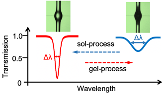
Label-free microcavity sensors have attracted much attention because they are critical to applications in medicine, environment, and security. Benefieting from high-Q factors and very small mode volumes of optical modes, single-nanoparticle detection can be achieved by monitoring the frequency shift, mode splitting, or linewidth broadening. In our experiment, an ultrahigh Q-factor microbubble resonator-based sensor is used to characterize dynamic phase transition of a thermosensitive hydrogel. By monitoring resonance wavelength shift and linewidth broadening, we (for the first time to our knowledge) reveal that the refractive index is increased and light scattering is enhanced simultaneously during the hydrogel hydrophobic transition process.
THz metasurfaces and devices
Terahertz (THz) metasurfaces have attracted significant interest because of their potential applications in biological medicine, detection, security imaging, and high-speed wireless communication. As the two-dimensional equivalent of metamaterials, metasurfaces respond to the incident radiation mainly through their geometrical patterns. Therefore, different terahertz devices have been proposed to expand the application of terahertz wave. In our experiment, we experimentally demonstrated a multi-resonance and ultra-wideband terahertz metasurface absorber, the maximum absorption rate of up to 92.5% at 0.745 THz. And, 90% absorption bandwidth beyond 1.2 THz can be observed with a central frequency of 1.8 THz. In addition, terahertz metasurface tunable resonators have also been achieved based on deep silicon etch.
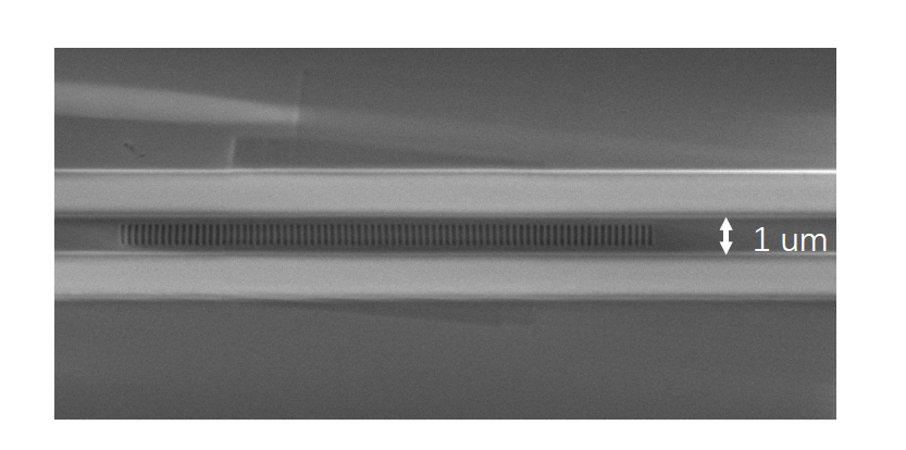
Photonic crystal nanobeam cavity devices
Silicon photonic crystal nanobeam cavity (PCNC) is considered as an ideal platform for on-chip integration, owing to the advantages of ultracompact footprint, enhanced light-matter interactions, high integrability with optical waveguides/circuits, and compatibility with CMOS processes. To date, various optical devices based on PCNC have been demonstrated, such as optical filters, lasers, photodetectors, electro-optical modulators, and electro-optical switches. By incorporating these silicon photonic devices, versatile and reconfigurable photonic networks can be realized. Thus, PCNC-based devices in near infrared wavelengths could be potentially important for future on-chip integrated silicon photonics.